Adding PCIe support and bring up the boot splash screen to DM814x U-Boot
It is desirable to have some visual feedback to user during system boot up process especially if the system takes more than few seconds to boot. For the Linux based set-top box that boot to the main GUI menu may take considerable amount of time depending on the number of processes it needs to start. Some system may need to program the FPGA bitmask, bring up the networking processes or bring up some externally connected devices. These steps add up to the total system boot up time. For system with video support, it is a good practice to have video up as soon as possible so that the user would know that the system is working and it is in the process of booting up the system. This is commonly known as putting the boot splash screen during boot process.
The TI8148 has the integrated PCIe support in it. The TI OMAP DM814x/AM287x evaluation platform (TI8148 EVM) also comes with one PCIe connnector where the HBA can be attached; however, the TI's official released u-boot-2010.06-psp04.00.01 does not have PCIe support enable. The board that I am using for this demonstration is the derivation of TI EVM board having a proprietary PCIe based video processor chips built in to the system. The video processor chip is capable of processing 4K-3D video. It has two HDMI ports and it has the built-in video/audio processing unit. This post is not about the integrated HDVPSS.
In order to put the splash screen at u-boot level, I have to do these things,
Initialize PCIe PLL clocks subsytem.
Initialize PCIe RC (Root Complex).
Initialize the video processor HDMI subsystem.
Put up the splash screen with logo and status bar.
Initialize the PCIe PLL
In reference to u-boot-2010.06-psp04.04.00.01 of EZSDK, the file board/ti/ti8148/evm.c has function pcie_pll_config() disable (commented out). It is understandable that the original author exercised the practice of not leaving free-running clock enable if no device was using it. Since I will be using it, this function need to be enable to configure PCIE's PLL clock in the control module (section 3 and 19.2.1 of [1]). The registers to be configured are PLLCFG0 to PLLCFG4 of the PCIe control module (base offset is 4814_0000). I made some minor change for the board I am using, enabling MEAS and enabling latch (50%).
static void pcie_pll_config()
{
        ..
        __raw_writel(0x70007017, PCIE_PLLCFG0); //per 19.3.1.1.1 sprugz8b.pdf manual.
        /*wait for ADPLL lock*/
        ..
}
at the end of pcie_pll_config(), wait for PLL to phase-lock by polling PLLSTATUS bit 1. Also a call to the function should be made in prcm_init(). This portion of code is only to configure PLL, feeding clock to the PCIe subsytem. It is the first step to be done before configuring/enumeratating the PCIe device. This PCIe PLL configuration must be done before the complete powerup sequence before the clock module is locked out so it is made as part of SBL ie.. (min_config).
Initialize PCIe Root Complex
The PCIe configuration registers of this OMAP SoC start at 5100_0000. The PCIe module is based on Synopsis Designware Core (DWC) and TI SERDES PHY. It can operate in either endpoint (EP) or root complex (RC). The mode to be initialized for this purpose is RC mode. To do this is to set RC mode(2) for PCIE_CFG(480h) of the control module, bring PCIe out of reset sequence and enable PCIe clock ( CM_DEFAULT_PCI_CLKCTRL, section 2.10.7 of [1]). Once the PCIe is out of stand-by mode, the PCIe link can be trained or set-up. Because the PCIe module of this SoC is single lane (x1), the PCIe is configured for x1 before link training is initiated. When link training is completed, the PCIe is configured as bridge device with outbound transaction set for base address 2000_0000 (refers to 2.12.1 of [4]). Some part of the code,
The mapped BAR, 2000_0000 is the 256MB address space set aside for PCIe device's use [4]. This is corresponded to the address of the downstream PCIe video chip. Accessing this address space after the mapping is to access the video processor chip (below snippet). For system with more than one PCIe devices, extra code for buses enumeration is needed. Shown here is for the simplest case, single PCIe device [6].
The next step is to set up the PCI header structure of u-boot so that it can be accessible by its drivers and utility. This includes registering PCI device, its respective read/write configuration space handlers etc.. Post enumeration is to set up the inbound transaction address space which is the local system memory space of the system.
When all is done with PCIe device configuration, the device's PCIe memory mapped address space can be dumped with u-boot's md command. Sample below is the content of the video processor control registers area.
TI-MIN#md 20000000
20000000: 00000000 00000000 00000000 00000000    ................
20000010: 00000000 00000000 00000000 00000000    ................
20000020: 00000000 00000000 00000000 00000000    ................
20000030: 00000000 00000000 00000000 00000035    ............5...
20000040: 000003e7 0000000e 0000000f 00000000    ................
20000050: 00000000 00000011 00000035 000003e7    ........5.......
20000060: 0000000e 0000000f 00000000 00000000    ................
TI document section 19.3.1 [1] describes all the necessary steps needed to set up the RC mode for this module. Initialization of PCIESS for the boot code or the high level kernel OS takes the exact same steps. In fact, I ported part of the code from the linux kernel originally done by TI [3] in linux-2.6,37-psp04.04.00.01/mach-omap2/pcie-ti81xx.c.
Initialize the video processor's HDMI subsystem
From this point onward, the PCIe video processor is accessible by u-boot. The proprietary video processor used in this derived platform has external DDR3 video display memory that need to be configured. The first step in this process is to set up its PLL clocks subsystem and set up its DDR3 memory controller (DDR training). Video PLL clock and audio PLL clock are set up as part of this initialization. Following this step, the EDID is read from the connected display device (monitor/tv) so that it can setup the HDMI interface correctly. My board's HDMI is connected to ASUS LCD monitor.
The information from EDID is used for configuring the HDMI [5] to match the capability of the display unit (TV/monitor) so that the splash screen will be properly centered. The gamma LUT, chroma scaler, dithering frame dimension, info frame, color space etc.. for the video pipe and the HDMI component of the video processor are then initialized accordingly.
Put up splash screen logo
The final step is to load the video pixels of the splash screen. One is static logo image and one is the progressive status bar. The logo image that is compiled along u-boot code (~100k) is then DMAed by the video processor to its layered output display memory buffer, the main display buffer. The overlay progressive status bar is output in the same way, but to its OSD display buffer and having its progress status update mechanism hooks up to the timer tick in order to update the progress bar. This part of putting the splash screen is the proprietary part that I cannot include any snippet due to NDA.
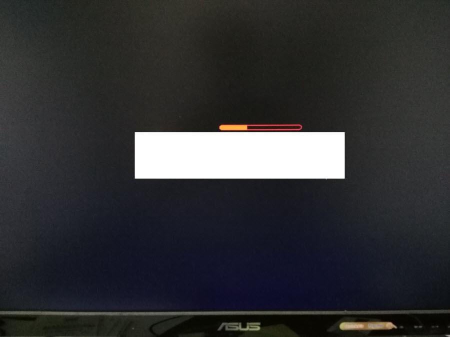
Splash screen with a progressing status bar (company logo blocked out).
Conclusion
It takes a little bit of effort to get this done, coding and debugging, but some lessons are learned during the process.
Citations
- 1
-
TMS320DM814x Davinci Digital Video Processor Technical Reference Manual, SPRUGZ8D, Revised April 2013.
- 2
-
arm-2009q1-203-arm-none-linux-gnueabi.bin, TI cross toolchain.
- 3
-
LINUXEZSDK-DAVINCI: Linux EZ Software Development Kit (EZSDK) for DM814x and DM816x- ALPHA,ezsdk_dm814x-evm_5_05_01_04_setuplinux, www.ti.com/tool/linuxezsdk-davinci, v5.05.01.04-ALPHA, 10 OCt, 2012.
- 4
-
TMS320DM8148, TMS320DM8148, TMS320DM8146, SPRS647D-MARCH 2011-REVISED SEPTEMBER 2012.
- 5
-
High Definition Multimedia Interface, Specification Version 1.3a, November 10, 2006
- 6
-
PCI Express System Architecture, MindShare Inc, Addison Wesley, ISBN: 0-321-15630-7, September 04, 2003.