Displaying Xilinx XADC on VGA
My previous blog was about displaying simple bar graph on a standard VGA 640x480@60HZ monitor using synthesized Verilog code. This blog is to follow on with that exercise, but using the actual sampled data from the Xilinx XADC instead.
The Artix7 FPGA on Digilent Nexys4DDR has a dual 12-bit 1 MPBS Analog-to-Digital converter in it which I think is pretty good enough for the wide variety of applications. According to its user guide 1, this integrated component is available in several Xilinx FPGA products. My understanding about its functionality would eventually be applicable to other Xilinx's FPGAs such as the Kintex, Zynq-7000 etc.. Later on I will use it with the Zynq-7000 series with the integrated ARM Cortex.
This XADC can access up to 16 auxiliary analog input channels. This is stated in page 17 of its user guide 1. For my exercise I will use only one bipolar pair of Vp/Vn input channels of this device. The nominal input range to this ADC channel will be in accordance to its specification which is 0-1V.
Tools and equipment use
Xilinx Vivado 2015.4
Digilent Nexys4DDR
Arbitrary waveform generator
VGA monitor
Cables
Implementation
Unfortunately I will have to make use of the Xilinx IP core for the XADC. Generate and instantiate it then feed its output to the VGA display monitor. I do not know its core well enough to do it with pure Verilog code. Even if I do it may not worth the effort.
The interfaces
In this implementation, the XADC is to be operated in Single Channel mode on channel 19 (VAUXP[3], VAUXN[3]). Its timing mode is continuous mode and its conversion rate is set to 500 KSPS. It is instantiated from the generated core IP.
The two bipolar inputs are from PMOD JXADC pin 1 (AD3P) and pin 7 (AD3N). The two inputs are connected to waveform generator during the test.
The output of XADC is stored in DPRAM location on XADC's EOC signal by its DRDY_OUT. Its EOC_OUT is connected to DEN_IN for continuous sampling.
SW[0] is use as sampling on/off switch. If SW[0]=1, sampled data is continously stored and displayed otherwise it displayed the previous sampled data. Basically I use it to take a snapshot of the sampled data.
The LED displays are not very useful other than to display the activity.
VGA plot the sampled point corresponded to the stored sampled data, xadc_data which is scaled value of the actual 12-bit data.
Code that generates VGA display signal and the related DPRAM access was described in my previous post. In this exercise, I only bring in those modules fnd instantiate them for this exercise.
Test
I use the output of the waveform generator to connect to the XADC channel 19 input. I take the snapshot photos of the sampled for the sine waveform and the ramp waveform as they are displayed on the VGA monitor below.
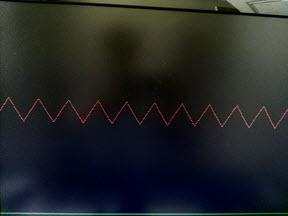
Image of the sampled 10KHZ ramp waveform, 1VPP
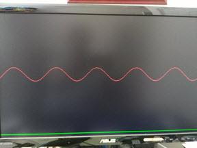
Image of the sampled 4KHZ sine waveform, 1VPP
The images above are the snapshots of the sampled waveforms resulting from the toggling of SW[0] that start/stop data storing process. The sampling process is continuous, only the storing process is controlled by SW[0].
Not much information from the LED displays since the data rate is much too fast to capture and the forever changing data output to the LED display make them stay lit.
Conclusion
It looks like the XADC is working for me. It took me a while to figure out and tuning the parameter especially when plotting in on the screen. My sample code is in https://github.com/souktha/vga_display_xadc. Source code includes a tcl script. By running the setup script it will create the workspace and run everything to generate the FPGA bitstream.